MCS-012 is an essential course in IGNOU‘s BCA program. This course explores the nuances of programming in assembly language as well as the basic ideas of computer organization. It seeks to provide students a thorough understanding of how computer systems work at the hardware level and how to communicate directly with hardware using assembly language.

Course Goals
Acquire an understanding of computer architecture to gain insight into the architecture of computer systems, including input/output systems, memory hierarchy, CPU, and data representation.
Acquire the skill of writing and debugging assembly language programs, which are essential for low-level programming jobs. Learn Assembly Language.
Investigate Machine-Level Operations: Learn how the CPU carries out commands from high-level programming languages by translating them into machine code.
Practical Skills: Gain practical experience through laboratory work and practical tasks, which support the course’s academic concepts.
Introduction to MCS-012: Computer Organisation and Assembly Language Programming
The Indira Gandhi National Open University (IGNOU) offers a Bachelor of Computer Applications (BCA) degree that aims to give students a strong foundation in computer science and information technology. MCS-012: Computer Organization and Assembly Language Programming stands out as a crucial course among the program’s varied offerings. The purpose of this painstakingly designed course is to familiarize students with the basic concepts of computer organization so they may understand the complex hardware operations of computer systems.
Understanding the fundamentals of computer architecture, such as the layout and operation of the central processor unit (CPU), memory hierarchy, and input/output systems, can be gained through MCS-012. The course also covers assembly language programming in great detail. Assembly language is a low-level programming language that gives you direct control over the hardware. Students who become proficient in assembly language may create programs that carry out operations at a fine level, which improves their capacity to efficiently optimize and debug systems.
Understanding the Importance of MCS-012 Short Notes:
1. Overview : Brief notes reduce an extensive amount of material into essential ideas and points. They offer a rapid and effective means of studying the key subjects in advance of the examination.
2. Focus on the Essentials: You may focus on each topic’s key elements by summarizing the available information. This guarantees that you cover the most relevant subjects and helps in setting priorities for your study materials.
3. Improved Retention: Taking quick notes requires you to take an active role with the information. Compared to passive reading, active learning promotes improved understanding and retention of knowledge.
4. Quick Reference: Brief notes are a quick reference that come in helpful when making last-minute changes. To fast brush up on specific concepts or formulas, you can swiftly scan them.
5. Time management: You may cover a lot of ground in less time by taking brief notes. This is very helpful if you don’t have much time to study before the test.
Most Repeated MCS-012 Important Questions for IGNOU BCA Exams Semester Wise :
BLOCK-1
Question 1: What is Von-Neumann architecture?
The Von-Neumann architecture, also known as the Von-Neumann model, is a computer architecture design concept proposed by mathematician and physicist John von Neumann in the 1940s. It is the basis for most computer systems in use today. The key features of the Von-Neumann architecture are:
- Stored-Program Concept: The instructions and data are stored in the same memory space. This allows programs to be modified by other programs, enhancing flexibility.
- Single Memory Space: Both data and instructions are stored in a single read-write memory.
- Sequential Execution: Instructions are executed sequentially unless a jump or branch instruction changes the order of execution.
- Four Main Components:
- Central Processing Unit (CPU): Contains the control unit (CU) and arithmetic logic unit (ALU), which perform calculations and control the execution of instructions.
- Memory: Stores data and instructions.
- Input/Output (I/O): Interfaces for external devices to communicate with the computer.
- Bus System: A communication system that transfers data between components of a computer.
The architecture forms the foundation of most modern computers, enabling them to perform a wide range of tasks by loading and executing stored programs.
Question 2: Explain the use of PC, IR, AC, MBR registers of the computer system.
- Program Counter (PC):
- The PC is a register in the CPU that contains the address of the next instruction to be executed.
- It is automatically incremented after each instruction fetch, ensuring that instructions are executed in sequence.
- During a jump or branch operation, the PC is updated with the address of the target instruction.
- Instruction Register (IR):
- The IR holds the currently executing instruction.
- When an instruction is fetched from memory, it is loaded into the IR.
- The control unit decodes the instruction in the IR to determine the required operations.
- Accumulator (AC):
- The AC is a general-purpose register used in arithmetic and logic operations.
- It temporarily holds data and intermediate results during calculations.
- For example, the result of an addition operation might be stored in the AC.
- Memory Buffer Register (MBR):
- The MBR, also known as the Memory Data Register (MDR), holds the data being transferred to or from memory.
- When data is read from memory, it is first loaded into the MBR before being used by the CPU.
- Similarly, when data is written to memory, it is loaded into the MBR before being transferred to the memory location.
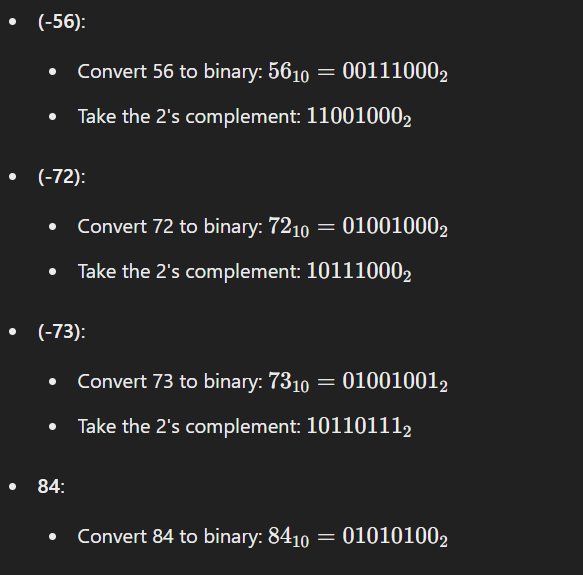
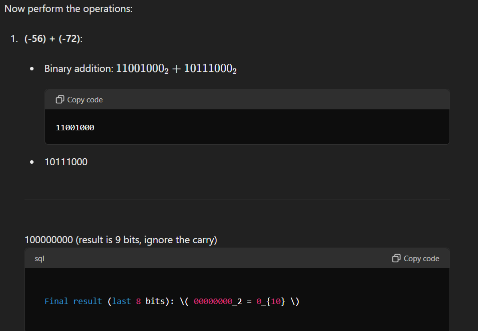
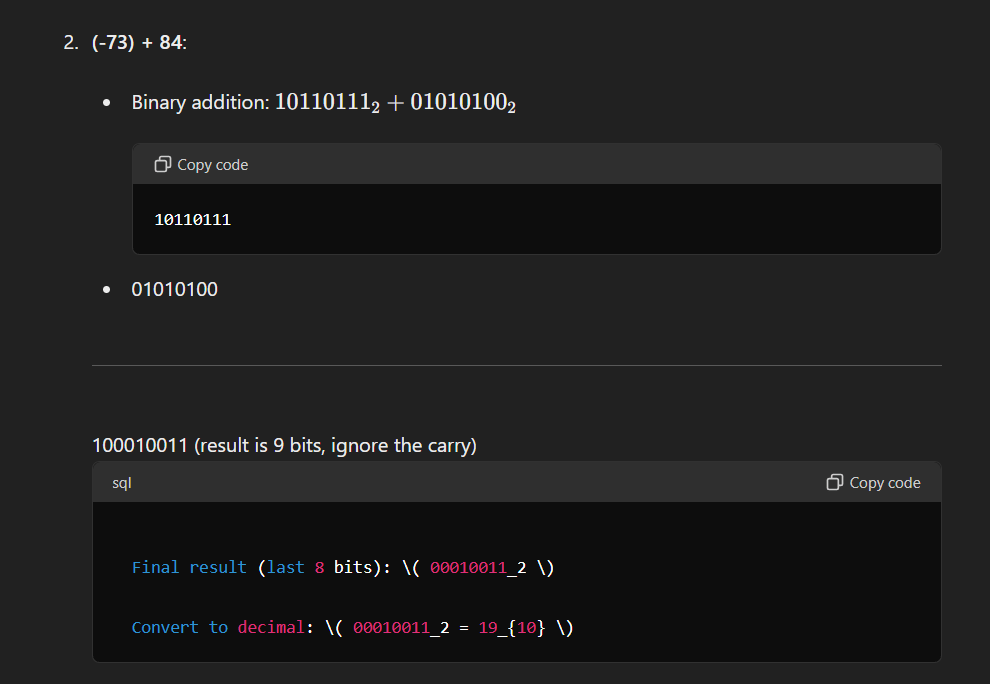
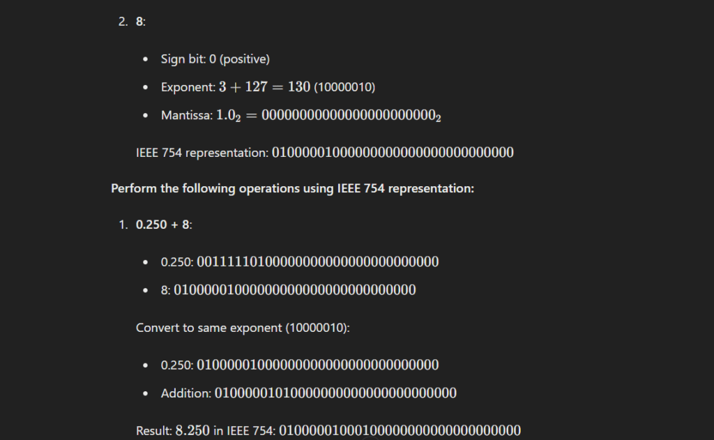
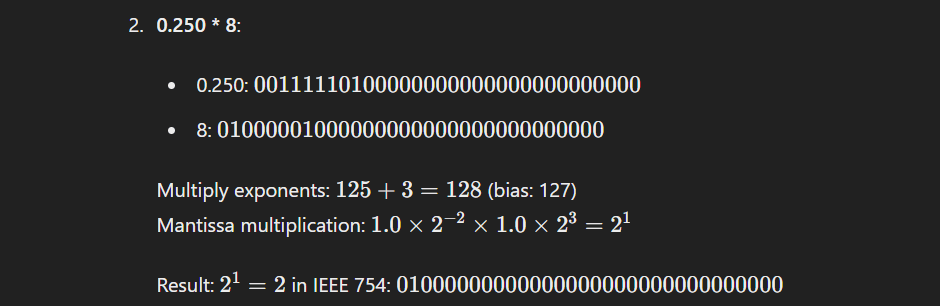
Question 3: Perform the following operations using 8-bit signed 2’s complement notation.
To perform the given operations, we first need to represent the numbers in 8-bit signed 2’s complement form:

Question 5: Explain the use of parity bit in error detection and correction code with the help of an example using an odd parity scheme?
A parity bit is a simple error detection mechanism used to ensure data integrity in digital communication systems. It involves adding an extra bit to a binary sequence to make the total number of 1’s either even (even parity) or odd (odd parity). The parity bit helps in detecting errors during data transmission.
Odd Parity Scheme: In an odd parity scheme, the parity bit is set such that the total number of 1’s in the binary sequence (including the parity bit) is odd.
Example: Consider a 7-bit binary data: 1011001.
- Count the number of 1’s in the data:
1011001has four 1’s.
- Determine the parity bit:
- Since the total number of 1’s (four) is even, we need to add a parity bit to make it odd.
- Parity bit = 1 (to make the total number of 1’s odd).
- Form the transmitted data:
- Original data:
1011001 - Parity bit:
1 - Transmitted data:
10110011
- Original data:
Error Detection: During transmission, if a single bit error occurs, the number of 1’s will change, and the parity will no longer be odd. This discrepancy indicates an error.
Example of Error Detection:
- Received data:
10110010 - Count the number of 1’s: There are five 1’s (odd parity is maintained).
- Since the parity is correct, no error is detected (in this example, the error might have affected a parity bit, or a multiple-bit error occurred, which is not detectable by a single parity bit).
Parity bits can detect single-bit errors effectively, but they cannot correct errors or detect multi-bit errors.
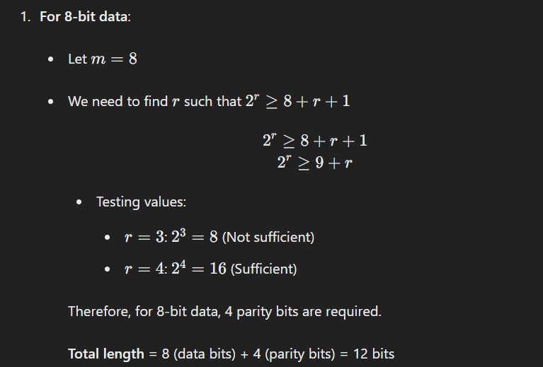
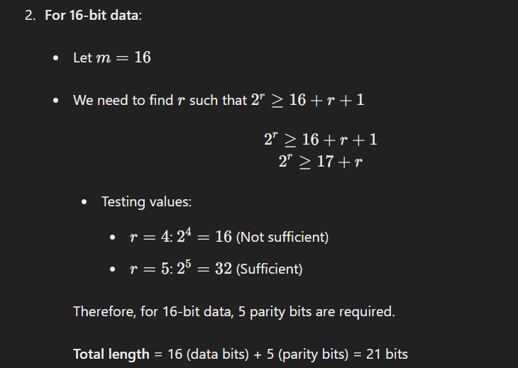
Question 6: Using Hamming code, what should be the length of the error detection code that detects the error in one bit for 8 and 16-bit data respectively?
Hamming Code: Hamming code is an error-detecting and error-correcting code that can detect up to two simultaneous bit errors and correct single-bit errors. The number of parity bits required is determined by the formula: 2r≥m+r+1 where r is the number of parity bits, and mmm is the number of data bits.
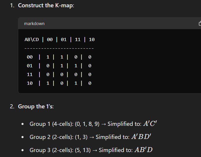
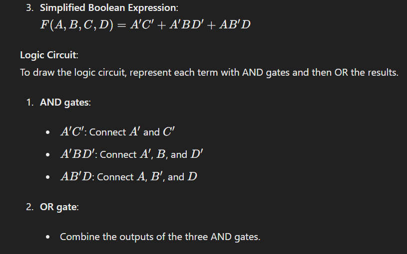
Question 7: Simplify the following using Karnaugh’s map (K-map)?
F (A, B, C, D) = Σ(0, 1, 3, 5, 8, 10, 13) Also, draw the logic circuit for the simplified expression.
Karnaugh Map (K-map) simplification:
Question 8: Explain the design of a 4×1 multiplexer?
A 4×1 multiplexer (MUX) selects one of four input data lines and forwards the selected input to a single output line based on the values of two select lines.
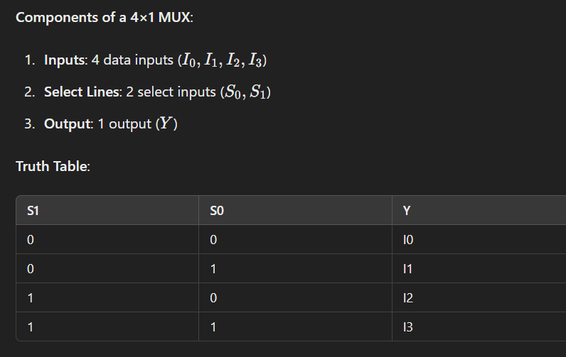
Design:
- Use four AND gates to combine each input with the appropriate combination of select lines.
- Use an OR gate to combine the outputs of the four AND gates.
Y=S1′ S0′ I0+S1′ S0 ‘I1+S1’S0′I2+S1’S0’I3
Question 9: Explain the construction of a full adder using a half adder?
A full adder adds three bits: two significant bits and a carry-in bit, producing a sum and a carry-out.
Components:
- Half Adder: Adds two bits, producing a sum and carry.
- Full Adder: Combines two half adders to add three bits.
Construction:
- First Half Adder:
- Inputs: AAA and BBB
- Outputs: S1 (sum) and C1 (carry)
- Second Half Adder:
- Inputs: S1 and Cin (carry-in)
- Outputs: S2 (final sum) and C2 (carry)
- OR Gate:
- Combines C1 and C2 to produce the final carry-out (Cout)
Logic Diagram:
- First Half Adder:
- Sum: S1=A⊕B
- Carry: C1=A⋅B
- Second Half Adder:
- Sum: S2=S1⊕Cin
- Carry: C2=S1⋅Cin
- OR Gate:
- Cout=C1+C2
JK Flip-Flop: A JK flip-flop is a type of flip-flop with two inputs, J and K, which can set, reset, or toggle the output based on the input values and the clock signal.
D Flip-Flop: A D flip-flop, or data flip-flop, has a single input (D)
BLOCK-2
Question 1: How many RAM chips of size 512 * 8 bit are needed to design a memory of 1M * 32bit?
To design a memory of 1M * 32-bit using RAM chips of size 512 * 8-bit, we need to determine the total number of such RAM chips required.
Calculation:
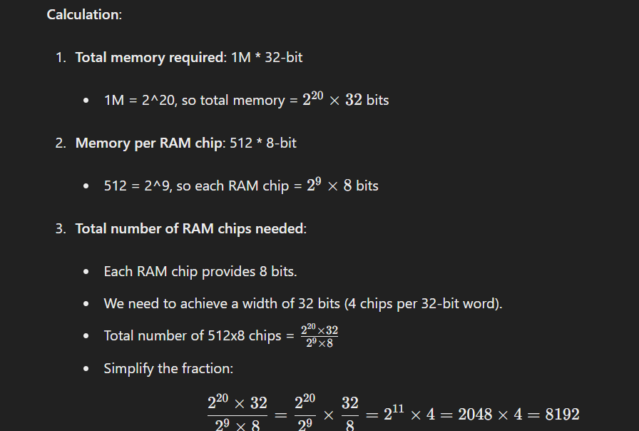
Therefore, 8192 RAM chips of size 512×8-bit are needed.
Question 2: What is RAID? List three features of RAID level 3?
RAID (Redundant Array of Independent Disks): RAID is a data storage virtualization technology that combines multiple physical disk drive components into one or more logical units for the purposes of data redundancy, performance improvement, or both. RAID levels use different architectures to balance these goals.
RAID Level 3: RAID 3 uses byte-level striping with a dedicated parity disk. Data blocks are striped across all disks in the array, with one disk dedicated to storing parity information. This configuration provides high data transfer rates and some level of redundancy.
Three Features of RAID Level 3:
- Byte-Level Striping: Data is striped at the byte level across multiple disks, improving the data transfer rate as multiple disks work in parallel to read/write data.
- Dedicated Parity Disk: A single disk is dedicated to storing parity information, which can be used to reconstruct data in case of a single disk failure.
- High Throughput: Ideal for applications that require high throughput for large data transfers, such as video streaming or large file processing, due to the parallel data transfer across multiple disks.
Question 3: Explain the programmed I/O with the help of a flow chart?
Programmed I/O: Programmed I/O is a method of data transfer where the CPU is responsible for moving data between I/O devices and memory. The CPU executes a program that checks the status of the I/O device, transfers data, and then proceeds with other tasks.
Flow Chart:
- Start
- Initialize I/O Device
- Check I/O Device Status:
- If device is not ready, repeat checking.
- If device is ready, proceed to next step.
- Transfer Data:
- Read data from device or write data to device.
- Check for End of Data Transfer:
- If data transfer is not complete, repeat from step 3.
- If data transfer is complete, proceed to next step.
- Terminate I/O Operation
- End
Start | Initialize I/O Device | Check I/O Device Status <---| | | | (Not Ready) | | | V (Ready) | Transfer Data | | | Check for End of Data Transfer | | | (Not Complete) | | | V (Complete) | Terminate I/O Operation | | End
Question 4: What is DMA? Draw and explain the block diagram of a DMA controller?
Direct Memory Access (DMA): DMA is a feature that allows I/O devices to directly transfer data to and from memory without the continuous involvement of the CPU. This improves the efficiency of data transfers and allows the CPU to perform other tasks while the transfer is ongoing.
Block Diagram of DMA Controller:
+---------------------+ | DMA Controller | +---------------------+ | Address Register | | Data Register | | Control Register | | Status Register | +---------------------+ | | +-----------------+ +-----------------+ | | | Memory Bus I/O Device CPU Bus
Explanation:
- Address Register: Holds the address of the memory location where data is to be transferred.
- Data Register: Temporarily holds the data being transferred between the memory and the I/O device.
- Control Register: Contains control information such as transfer direction (read or write), transfer mode, and other control signals.
- Status Register: Indicates the status of the DMA transfer, such as transfer complete or error status.
- Memory Bus: Connects the DMA controller to the system memory.
- I/O Device: The device involved in the data transfer.
- CPU Bus: Allows the CPU to communicate with the DMA controller for configuration and control.
Operation:
- The CPU initializes the DMA controller by writing the necessary parameters (memory address, data count, transfer direction) to the control and address registers.
- The DMA controller takes over the bus and transfers data directly between the memory and the I/O device.
- Once the transfer is complete, the DMA controller sends an interrupt signal to the CPU to indicate completion.
Question 5: Explain the working of CD-ROM and DVD-ROM with the help of a block diagram?
CD-ROM (Compact Disc Read-Only Memory): CD-ROM is a type of optical disc that stores data that can be read but not written or erased. It uses a laser to read data encoded as tiny pits on the surface of the disc.
Block Diagram of CD-ROM:
+--------------------+ | CD-ROM Drive | +--------------------+ | Laser Diode | | Photodiode | | Optical System | | Servo Mechanism | | Disc Motor | +--------------------+ | Interface | +-------------+ | Controller | +-------------+ | CPU/Memory
Explanation:
- Laser Diode: Emits a laser beam that is focused onto the surface of the disc.
- Photodiode: Detects the reflected laser beam and converts it into an electrical signal.
- Optical System: Focuses the laser beam onto the disc surface and guides the reflected light to the photodiode.
- Servo Mechanism: Adjusts the position of the laser to keep it focused on the data tracks.
- Disc Motor: Rotates the disc at a constant speed.
- Controller: Manages the interface between the CD-ROM drive and the computer, controlling data transfer and communication.
DVD-ROM (Digital Versatile Disc Read-Only Memory): DVD-ROM is an optical disc storage format that offers higher storage capacity than CD-ROM, using a similar technology but with denser data encoding and multiple layers.
Block Diagram of DVD-ROM:
+---------------------+ | DVD-ROM Drive | +---------------------+ | Laser Diode | | Photodiode | | Optical System | | Servo Mechanism | | Disc Motor | +---------------------+ | Interface | +-------------+ | Controller | +-------------+ | CPU/Memory
Explanation: The working of a DVD-ROM is similar to that of a CD-ROM but with some key differences:
- Higher Density: DVDs use a smaller laser wavelength and tighter track spacing to store more data.
- Multiple Layers: DVDs can have multiple layers of data storage, significantly increasing their capacity.
- Improved Error Correction: Enhanced error correction algorithms to ensure data integrity.
Both CD-ROM and DVD-ROM drives use lasers to read data encoded as pits and lands on the disc surface. The reflected laser beam is converted into an electrical signal by the photodiode, processed by the controller, and then sent to the computer for further use.
BLOCK-3
Ques. 1 Explain the Instruction Fetch with the help of micro-operations.
Instruction fetch is the process of retrieving an instruction from memory to be executed. This involves several steps, often broken down into smaller operations called micro-operations. Here’s an overview of the instruction fetch process using micro-operations:
- PC (Program Counter) Setup:
MAR <- PC: The contents of the Program Counter (PC) are loaded into the Memory Address Register (MAR).
- Memory Read:
MDR <- Memory[MAR]: The memory location pointed to by MAR is read, and the contents are placed into the Memory Data Register (MDR).
- Increment PC:
PC <- PC + 1: The PC is incremented to point to the next instruction.
- Instruction Register Load:
IR <- MDR: The contents of the MDR (which hold the fetched instruction) are loaded into the Instruction Register (IR).
These steps are executed in a sequence to ensure the correct instruction is fetched from memory and prepared for decoding and execution.
Ques. 2 Determine the 8-bit values in registers after the execution of the following sequence of micro-operations: R1 <- R2 + R3 Exclusive OR. R1 + R2 – R3 Subtract R3 from R1.
Initial register values:
- R1 = 00001111
- R2 = 11110000
- R3 = 11001100
- R4 = 10101010
- Micro-operation 1: R1 <- R2 XOR R3
- R2: 11110000
- R3: 11001100
- XOR: 00111100 (R1 = 00111100)
- Micro-operation 2: R1 <- R1 + R2 – R3
- R1: 00111100
- R2: 11110000
- Addition: 00111100 + 11110000 = 10001100
- Subtract R3: 10001100 – 11001100 = 11000000 (R1 = 11000000)
- Micro-operation 3: Subtract R3 from R1 (R1 <- R1 – R3)
- R1: 11000000
- R3: 11001100
- Subtraction: 11000000 – 11001100 = 11110100 (R1 = 11110100)
Final values:
- R1 = 11110100
- R2 = 11110000
- R3 = 11001100
- R4 = 10101010
Ques. 3 Write a short note on instruction pipelining.
Instruction pipelining is a technique used in the design of modern microprocessors to improve their instruction throughput (the number of instructions that can be executed in a unit of time). It allows multiple instructions to be processed simultaneously by breaking down the execution pathway into distinct stages, each handled by a different part of the processor.
A typical instruction pipeline might consist of the following stages:
- Fetch: Retrieve the instruction from memory.
- Decode: Interpret the instruction to determine the required action.
- Execute: Perform the operation specified by the instruction.
- Memory Access: Read from or write to memory if needed.
- Write Back: Write the result of the operation back to a register.
Each stage processes part of an instruction and passes it to the next stage. While one instruction is being decoded, another can be fetched, and yet another can be executed. This parallelism increases the efficiency and speed of instruction execution.
Challenges in pipelining include handling data hazards, control hazards, and structural hazards, which can cause pipeline stalls and reduce performance. Techniques like instruction reordering, branch prediction, and out-of-order execution are often employed to mitigate these issues.
Ques. 4 List any three characteristics of RISC architecture.
- Simplicity of Instructions: RISC (Reduced Instruction Set Computer) architectures use a small, highly optimized set of instructions. Each instruction is designed to execute very quickly, typically in one clock cycle, making the pipeline more efficient and simpler to implement.
- Load/Store Architecture: RISC processors use a load/store architecture, where operations on data are performed only on CPU registers, and separate instructions are used for loading data from memory into registers and storing data back to memory. This separation simplifies instruction execution and enhances pipeline performance.
- Fixed Instruction Length: Instructions in a RISC architecture are typically of a fixed length, which simplifies the process of fetching, decoding, and executing instructions. This uniformity helps in faster instruction decoding and can improve the overall speed of instruction execution.
Ques. 1: Program in 8086 Assembly Language to Count Characters in a String
Here’s a simple program in 8086 assembly language that counts the number of characters in a string stored in the data segment. This program assumes the string is terminated by a null character (ASCII 0).
.model small
.stack 100h
.data
string db 'Hello, World!', 0 ; Define a string terminated by null character
.code
main proc
; Set up the data segment
mov ax, @data
mov ds, ax
; Initialize variables
lea si, string ; Load effective address of string into SI
mov cx, 0 ; Initialize counter to 0
count_loop:
lodsb ; Load byte at address DS:SI into AL, increment SI
cmp al, 0 ; Compare AL with 0 (null character)
je end_count ; If AL is 0, end of string is reached, jump to end_count inc cx ; Increment character count
jmp count_loop ; Repeat the loop
end_count:
; CX now contains the length of the string
; Terminate program (for DOS)
mov ah, 4Ch
int 21h
main endp
end main
Explanation:
- Data Segment Setup:
.model smallspecifies the memory model..stack 100hreserves 256 bytes for the stack..datadefines the data segment, where we store the string.
- Code Segment Setup:
mov ax, @dataandmov ds, axinitialize the data segment register.lea si, stringloads the effective address of the string into SI register.mov cx, 0initializes the counter CX to 0.
- Counting Loop:
lodsbloads the byte at DSinto AL and increments SI.cmp al, 0compares the loaded byte with the null character.je end_countjumps to end_count if the null character is found.inc cxincrements the counter if the character is not null.jmp count_looprepeats the loop for the next character.
- End Count:
- The length of the string is now in CX.
mov ah, 4Chandint 21hterminate the program.
Ques. 2: Use of Interrupt Vector Table (IVT) in Handling Interrupts for 8086 Microprocessor
The Interrupt Vector Table (IVT) is a critical component in the architecture of the 8086 microprocessor for handling interrupts. Here’s a discussion on its use and importance:
What is the Interrupt Vector Table (IVT)?
The IVT is a memory-resident table located at the beginning of the memory address space, from address 0000h to 03FFh. It consists of 256 entries, each entry being 4 bytes long, totaling 1 KB of memory.
Structure of IVT:
- Entries: Each entry in the IVT contains the segment address and the offset address of the interrupt service routine (ISR) for each interrupt vector.
- Addressing: The address of an ISR is stored as a far pointer (segment) which the CPU uses to jump to the appropriate ISR.
Handling Interrupts:
- Hardware Interrupts: These are generated by peripheral devices like the keyboard, mouse, or timer.
- When a hardware interrupt occurs, the device sends an interrupt request (IRQ) to the CPU.
- The CPU acknowledges the interrupt and looks up the corresponding ISR address in the IVT.
- Software Interrupts: These are generated by software instructions such as
INT n.- When a software interrupt instruction is executed, the CPU uses the interrupt number to index into the IVT.
- The CPU then fetches the ISR address from the IVT and transfers control to the ISR.
- Processing the Interrupt:
- The CPU saves the current execution context (registers and flags) on the stack.
- It then jumps to the ISR using the address obtained from the IVT.
- The ISR performs the required task and ends with an
IRETinstruction, which restores the saved context and resumes normal execution.
Importance of IVT:
- Efficient Interrupt Handling: The IVT allows for quick and efficient redirection of the CPU to the appropriate ISR without complex checking mechanisms.
- Scalability: The IVT supports up to 256 different interrupts, allowing a wide range of devices and software interrupts to be managed.
- Flexibility: The ISR addresses in the IVT can be dynamically modified, allowing the system to adapt to changing requirements and configurations.
Example:
For interrupt number 9 (keyboard interrupt), the IVT entry at address 0009h * 4 = 0024h would contain the segment and offset of the keyboard ISR.
Conclusion:
The IVT is a foundational mechanism for handling interrupts in the 8086 microprocessor, providing an organized and efficient way to manage both hardware and software interrupts. Its structure and functionality are essential for responsive and reliable system performance.
Download PDF Of Above Content In 3 Paper
Conclusion:
With these IGNOU MCS-012 BCA short notes, you’ll be well-equipped to tackle your exams with confidence. Remember to complement your study efforts with regular practice and mock tests. Good luck!


[…] Read More: MCS – 012(COMPUTER ORGANISATION & ASSEMBLY LANGUAGE) Important Short Notes| Expected Question … […]